 Veteran Owned
 Veteran Owned
Transparent Conductors
What is Measured
Delcom sensors can measure Transparent conducting materials (TCMs), Transparent Conducting Films (TCFs), Transparent Conducting Oxides (TCOs) and other materials to include:
- Indium tin oxide (ITO)
- Fluorine doped tin oxide (FTO)
- Doped zinc oxide, Indium Zinc Oxide (IZO)
- Aluminum Zinc Oxide (AZO)
- Gallium doped Zinc Oxide (GZO)
- Carbon nanotube (CNT) networks
- Graphene
- Poly(3,4-ethylenedioxythiophene) (PEDOT) Polymers and its derivatives
Similarly, Delcom sensors can measure TCMs created utilizing various material structures to achieve target transparency and conductivity to include:
- Thin films
- Metal grids
- Metal mesh
- Random metallic networks
- Nanowire meshes
- Ultra thin metal films
- Crackle networks
- Networks composed of metallic nanowires such as Ag, Au and Cu
Lastly, Delcom sensors are compatible with nearly all TMC and TCO manufacturing processes to include:
- Metal organic chemical vapor deposition (MOCVD),
- Metal organic molecular beam deposition (MOMBD),
- Solution deposition,
- Spray pyrolysis,
- Ultrasonic nozzle spray
- Pulsed laser deposition (PLD)
- Magnetron sputtering
- CNT growth, separation, and substrate application process
- Nano-wire synthesis
Why Measure with Delcom
The challenge faced by TCM materials is ensure the highest possible visual transmittance while minimizing sheet resistance. The conductivity of the material is nearly always directly related oxidation levels, dopant concentration, and thickness in the case of TCOs. In regards to meshes, nanowires, and grids, other factors such as patterns, the size of the particles, and the ability of particles to bond/fuse influence the conductivity of the material.
Figure 1: Transmittance vs. Sheet resistance
![]()
Traditionally, four point probes have been used to measure the sheet resistance of TCMs and TCOs. However, with Delcom’s eddy current technology, these materials can be measured inline and in situ without touching or destroying the material.
Delcom sensors offer the following advantages over four point probes:
- Is non-destructive
- Reads through insulating layers
- Measures moving material
- Provides nearly instantaneous readings
- Provides real-time process inspection
Not impeded by texture or patterns
Employment Strategies
All delcom sensors are available in a vacuum-ready configuration. Vacuum ready sensors are devoid of anodized materials, nickel coated hardware, and insulators that out-gas.
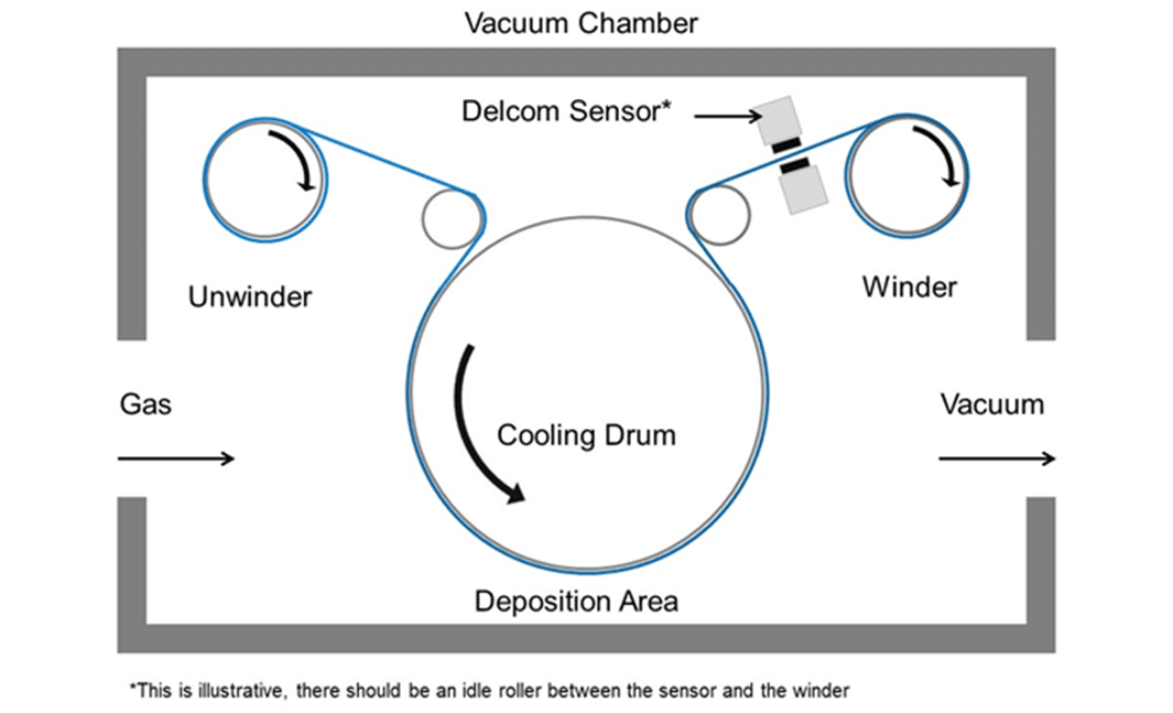
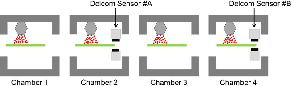
For in situ roll to roll process, the best placement for the Delcom sensor is inside the chamber just after the coating of the conductive material.
Figure 2: 20J3 Sensor Placed In Situ
For non-flexible substrates coated in vacuum (e.g. glass), the Delcom sensors should usually be placed inside the chamber immediately after the deposition process.
Figure 3: In Situ monitoring of vacuum coated glass
Cross-Web & Downstream Monitoring
In general, Delcom sensor deployment strategies can include one or more of the following deployment tactics.
|
Deployment Strategy |
Image | Advantages |
|---|---|---|
| Single sensor single spot | 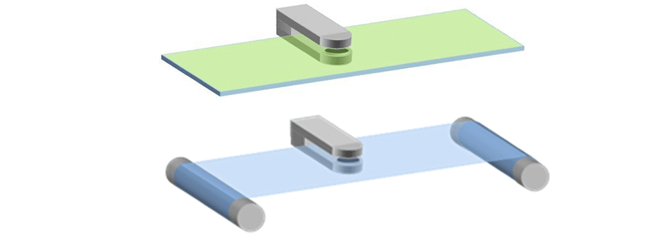 |
|
| Two sensors monitoring cross-web | 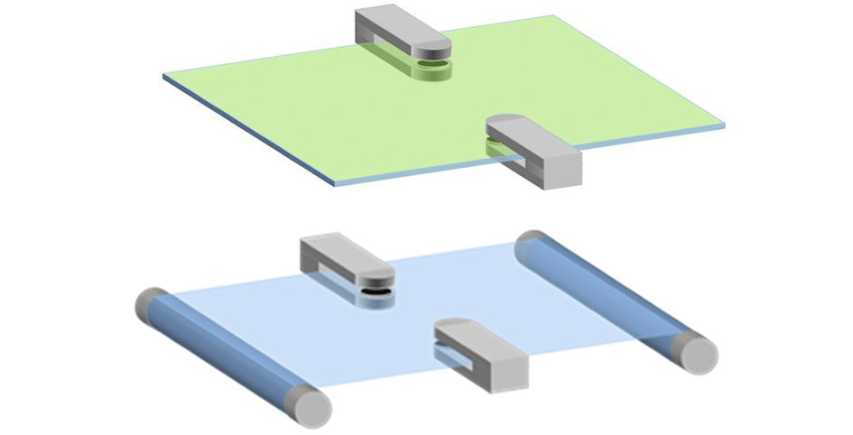 |
|
| Two sensors monitoring downstream | 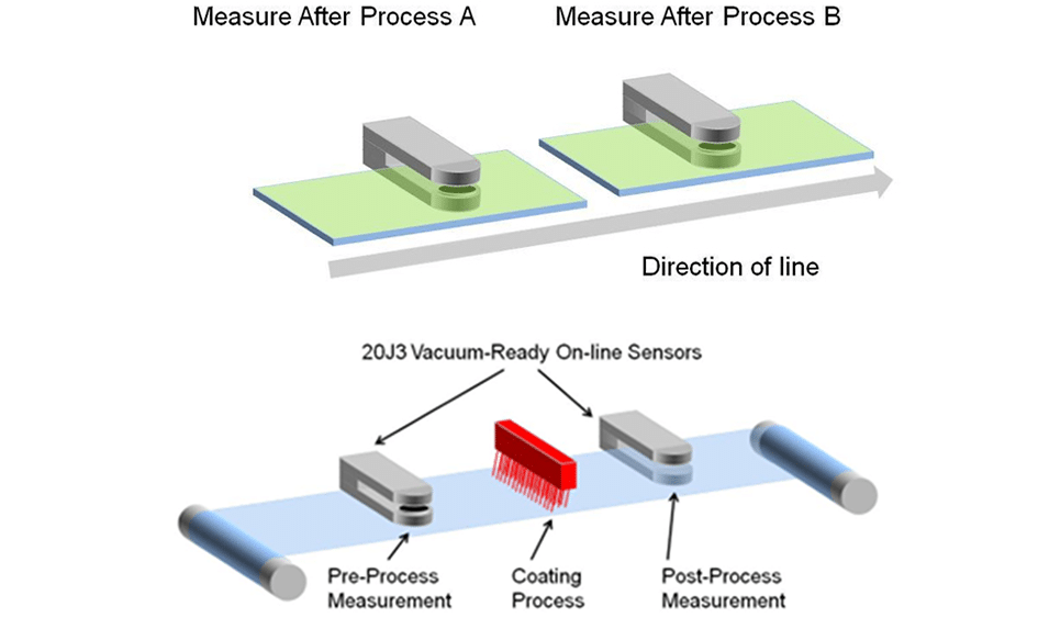 |
|
| Multi-channel monitoring cross-web | 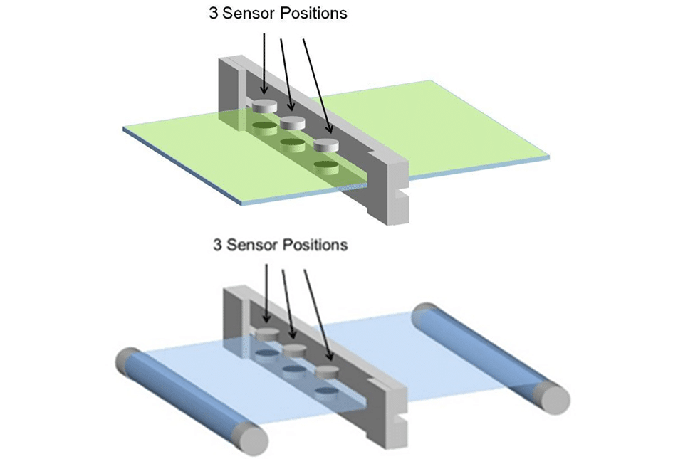 |
|
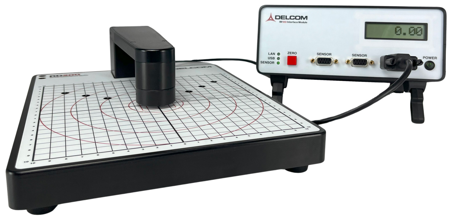
Recommended Sensors
Delcom recommends the following sensors based on the user’s material, stage of development, and application.
| Use case | Image | Recommended Sensor | Use case |
|---|---|---|---|
| Benchtop | 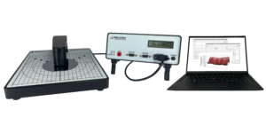 |
RD200 |
|
| Benchtop | 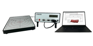 |
RS200 |
|
| Benchtop |  |
RD300 |
|
| Benchtop | 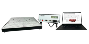 |
RS300 |
|
| Benchtop | 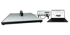 |
RD450 |
|
| Benchtop | 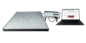 |
RS450 |
|
| Inline | 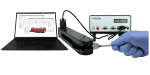 |
20J3 Hybrid |
|
| Inline | 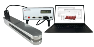 |
20J3 Inline |
|
| Inline | 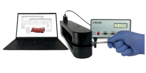 |
30C9 Hybrid |
|
| Inline | 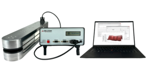 |
30C9 Inline |
|
| Inline | 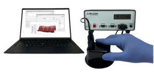 |
S3 Hybrid |
|
| Inline | 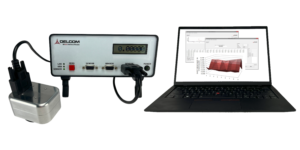 |
S3 Inline |
|
| Inline | 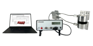 |
OEM |
|
| Inline | 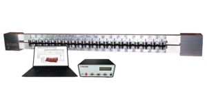 |
Multisensor |
|
Recommended Sensor Range
Typical sheet resistance for TCOs is 5 ohms/square to 500 ohms/square. Carbon Nanotubes (CNT) tend to come in with 90% transparency and around 100 ohms/square. Graphene can range from 30 ohms/square to 3,000 ohms/square. The values for common TCMs are listed in the chart below
Figure 4: possible transmittance and sheet resistance of common TCM materials
![]()
Delcom sensors measure sheet resistance. Delcom makes sensors in four ranges – each range able to measure a different range of sheet resistances. When considering which sensor is right for a particular application, the right range of instrument must be selected based on the target sheet resistance of the material.
Figure 5: Delcom’s sensor ranges:
| Range Name | Min Sheet Resistance in ohms/square |
Max Sheet Resistance in ohms/square |
|---|---|---|
| x10 | 5 | 100000 |
| x1 | 0.5 | 10000 |
| ÷10 | 0.05 | 1000 |
| ÷100 | 0.005 | 100 |
Given the typical target sheet resistance of between 5 and 500 ohms/square, the recommended instrument range for this application is “x10”. The x10 range instrument can measure from 5 ohms/square to 100,000 ohms per square.