 Veteran Owned
 Veteran Owned
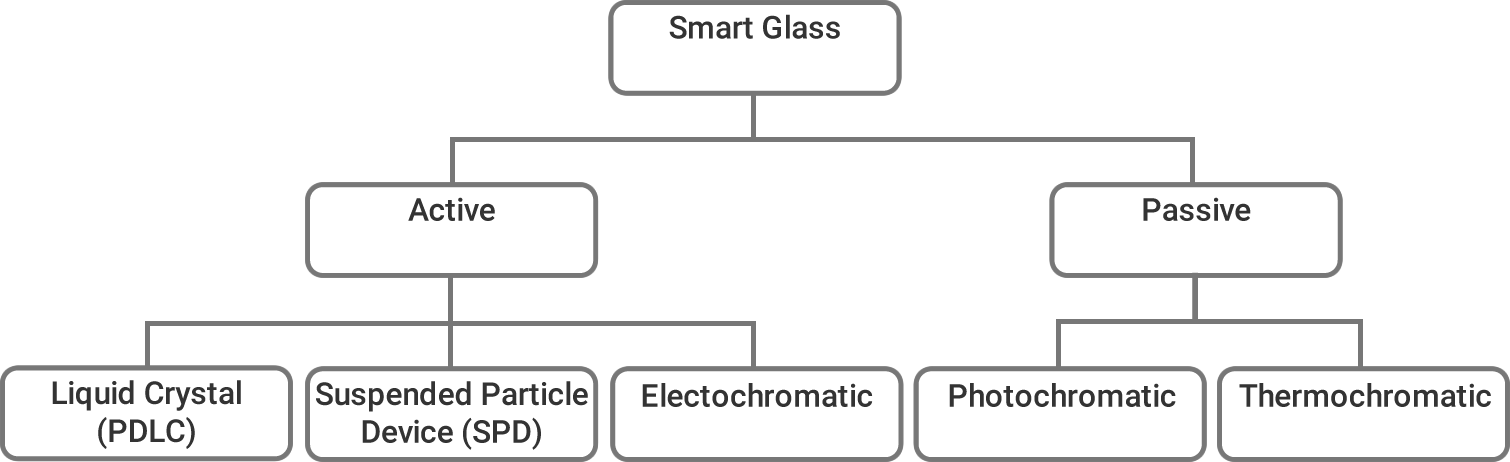
Smart Glass
What is Measured
Delcom sensors are regularly used to characterize the transparent conductor (TC) layer of both Photochromatic and Thermochromic smart glass*. However, this paper will focus primarily on the three primary types of active smart glass (PDLC, SPD, and Electrochromic/electrochromatic).
Figure 1: Types of smart glass
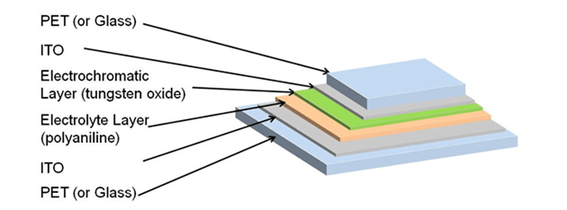
The three active smart glass technologies (PDLC, SPD, and Electrochromatic) have an active or smart layer that is a stack of material or coatings sandwiched between transparent layers of glass or plastic. The active portion of the stack has a transparent conductor (TC) on one side, material in the middle and a TC layer on the other side. The performance of the TC layer is critical as it is relied upon to alter the operating modes of the smart glass by applying a current/voltage between the two TC layers effecting an electromagnetic field on the material located between the two layers of the transparent conductor. It is this electromagnetic field that effects the liquid crystals (in the case of PDLC glass), rod-like suspended particles (in the case of SPD), lithium ions (in the case of electrochromatic glass).
Figure 2: PDLC Glass Cross-Section
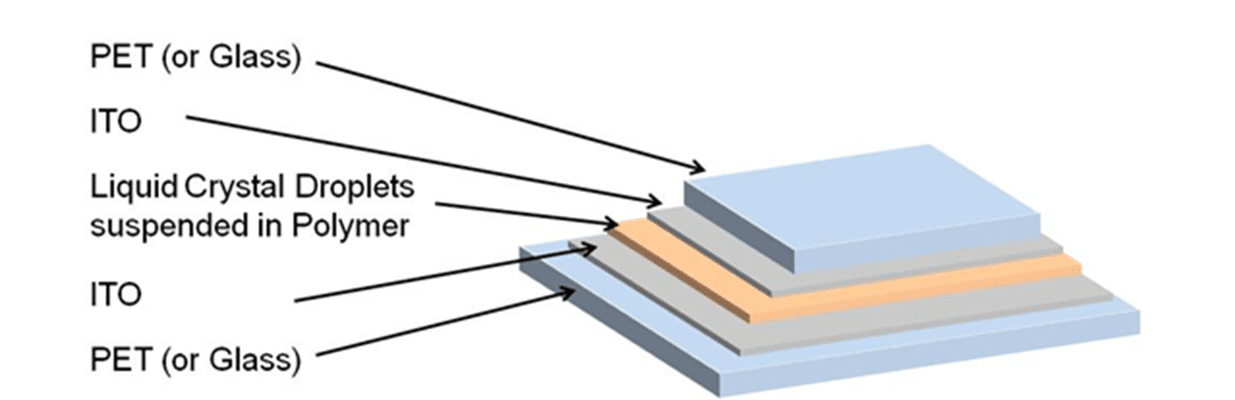
Figure 3: SPD Glass Cross-Section
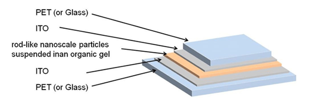
Figure 4: Electrochromatic Glass Cross-Section
Delcom sensors are used to characterize the two transparent conductor (TC) layers of the smart glass material “stack”. By ensuring the layers are within the target sheet resistance range and are free of defects, the researcher/manufacturer can ensure optimal performance of the smart glass product.
Delcom sensors can measure the transparent conductor (TC) layer of a smart glass product regardless of its composition to include:
- Tin-doped indium oxide (In2O3(Sn) (ITO)
- Antimony-doped or fluorine-doped tin oxide (SnO2:F)
- Aluminum-doped zinc oxide (ZnO:Al)
- TCC (transparent conductive coating) – thin metal layer(s) composed of Ag, Al, Pd, Cu, Pd, Pt, In, Mo, or Au
- Materials such as wire mesh, transparent and flexible electrodes (TFEs) such as Ag nanowires (NWs), graphene, carbon nanotubes, and conducting polymers etc.
Why Measure with Delcom
It is important to note that because eddy current meters rely on a magnetic field to achieve their reading, they have a number of advantages over four-point probes to include:
- Is non-destructive
- Reads through insulating layers
- Measures moving material
- Provides nearly instantaneous readings
- Provides real-time process inspection
Employment Strategies
All delcom sensors are available in a vacuum-ready configuration. Vacuum ready sensors are devoid of anodized materials, nickel coated hardware, and insulators that out-gas.
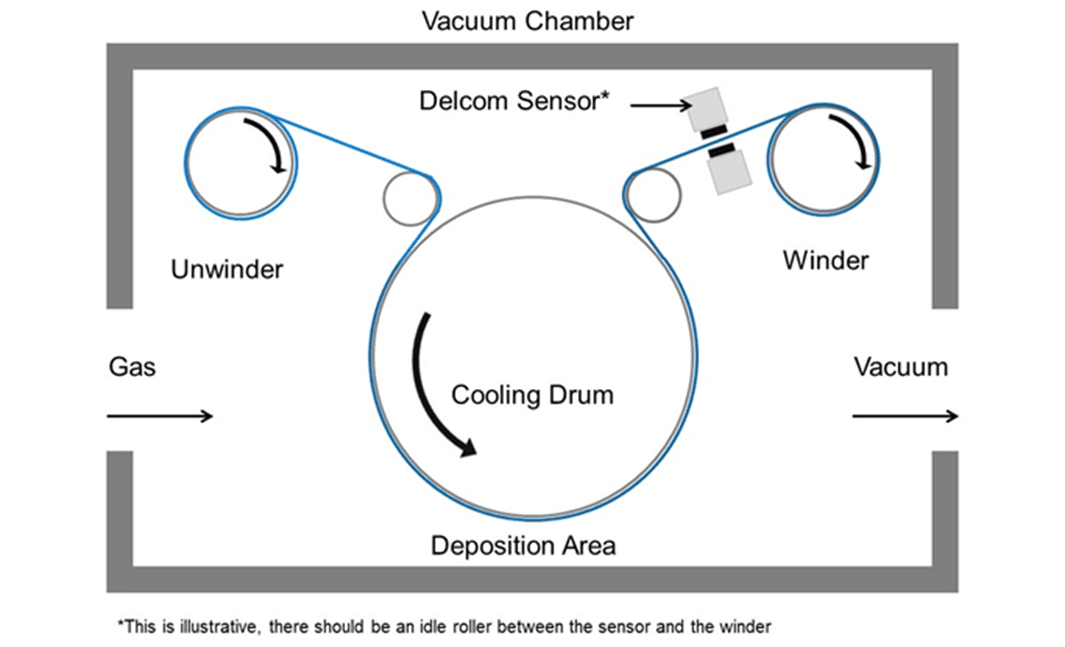
The coated glass should (ideally) be characterized immediately after the coating occurs to have the most “closed loop” process control feedback and impact. For in-situ manufacturing processes, the Delcom sensor should be placed in vacuum.
Figure 5: In situ monitoring for vacuum coated glass
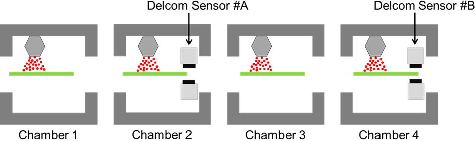
For in situ roll to roll process, the best placement for the Delcom sensor is inside the chamber just after the coating of the conductive material.
Figure 6: Delcom sensor monitoring roll to roll inline vacuum coating
Cross-Web & Downstream Monitoring
In general, Delcom sensor deployment strategies can include one or more of the following deployment tactics.
|
Deployment Strategy |
Image | Advantages |
|---|---|---|
| Single sensor single spot | 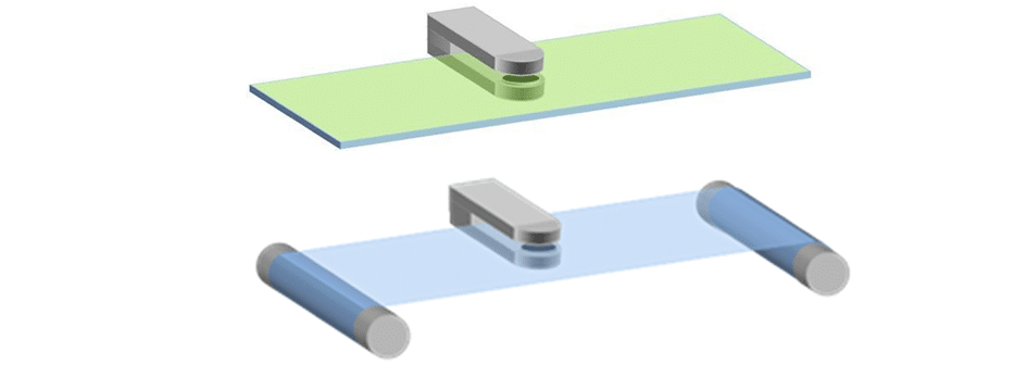 |
|
| Two sensors monitoring cross-web | 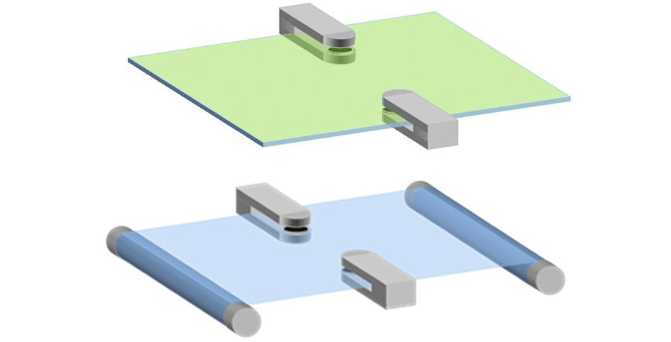 |
|
| Two sensors monitoring downstream |  |
|
| Multi-channel monitoring cross-web | 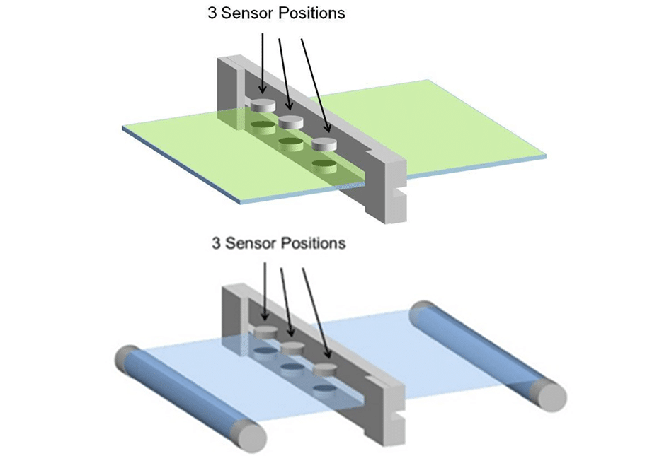 |
|
Recommended Sensors
Delcom recommends the following sensors based on the user’s material, stage of development, and application.
| Use case | Image | Recommended Sensor | Use case |
|---|---|---|---|
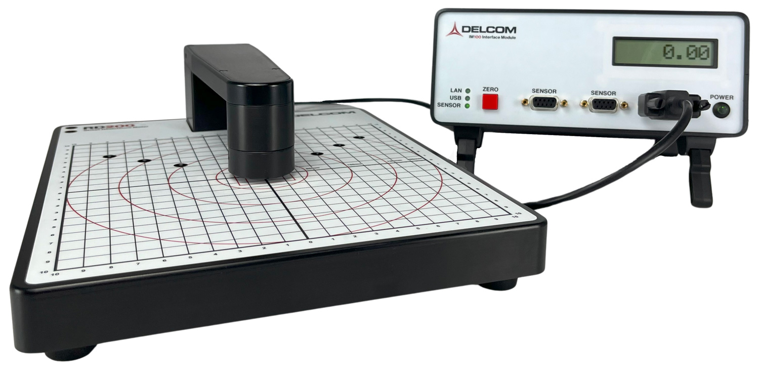
| Benchtop | 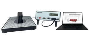 |
RD200 |
|
| Benchtop | 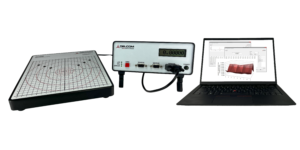 |
RS200 |
|
| Benchtop |  |
RD300 |
|
| Benchtop | 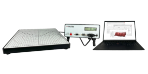 |
RS300 |
|
| Benchtop | 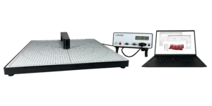 |
RD450 |
|
| Benchtop | 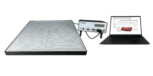 |
RS450 |
|
| Inline | 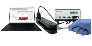 |
20J3 Hybrid |
|
| Inline | 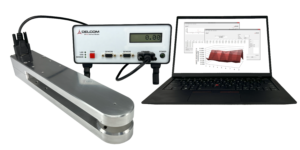 |
20J3 Inline |
|
| Inline |  |
30C9 Hybrid |
|
| Inline |  |
30C9 Inline |
|
| Inline |  |
S3 Hybrid |
|
| Inline |  |
S3 Inline |
|
| Inline | 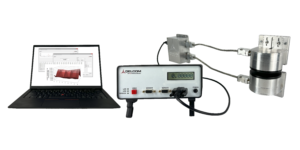 |
OEM |
|
| Inline | 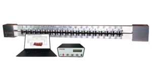 |
Multisensor |
|
Recommended Sensor Range
The most commonly used TC is ITO. The ITO layer is usually deposited in vacuum using a physical vapour deposition (PVD) method of direct current (DC) magnetron sputtering. The target resistance of each ITO layer is usually between 5 and 400 ohms per square.
Figure 7: Smart Glass Transparent Conductor Layers
| PDLC | SPD | Electrochromatic | |
|---|---|---|---|
| Manufacturing Method | enhanced cathodic sputtering, evaporation, sol-gel methods, or chemical vapor deposition (CVD) | enhanced cathodic sputtering, evaporation, sol-gel methods, or chemical vapor deposition (CVD) | enhanced cathodic sputtering, evaporation, sol-gel methods, or chemical vapor deposition (CVD) |
| Transparent Conductor Material | In2O3(Sn), SnO2:F), ZnO:Al | In2O3(Sn), SnO2:F), ZnO:Al | In2O3(Sn), SnO2:F), ZnO:Al |
| Substrate | Glass, polymer film, polyester film: polyethylene terephthalate (PET) | Glass, polymer film, polyester film: polyethylene terephthalate (PET) | Glass, polymer film, polyester film: polyethylene terephthalate (PET)) |
| TC Layer Thickness | from 50 to 100 nm | from 50 to 100 nm | 100 to 400 nm |
| Target Sheet resistance (in ohms/square) | 40 50 to 200 |
400 50 to 200 |
5-30 25 or less. |
Delcom sensors measure sheet resistance. Delcom makes sensors in four ranges – each range able to measure a different range of sheet resistances. When considering which sensor is right for a particular application, the right range of instrument must be selected based on the target sheet resistance of the material.
Figure 8: Delcom’s sensor ranges:
| Range Name | Min Sheet Resistance in ohms/square |
Max Sheet Resistance in ohms/square |
|---|---|---|
| x10 | 5 | 100000 |
| x1 | 0.5 | 10000 |
| ÷10 | 0.05 | 1000 |
| ÷100 | 0.005 | 100 |
Smart Glass products typically have a target sheet resistance of between 25 and 400 ohms/square. Therefore, the recommended instrument range for this application is “x10”. The x10 range instrument can measure from 5 ohms/square to 100,000 ohms per square.
*Synonyms for smart glass include: PDLC, Clear to Opaque Glass, Dimmable Glass, Dynamic Glass, Electrochromic Glass, Electrochromatic Glass, Electronic Glass, Intelligent Glass, LCD Glass, Light Control Glass, Liquid Crystal Glass, PDLC Glass, Privacy Glass, Self-Tinting Glass, Self-Tinting Windows, Smart Glass, Smart Tint, Smart Windows, Switch Glass, Switchable Glass, Switchable Smart Glass, Switchable Smart Film, and Tintable Glass.