 Veteran Owned
 Veteran Owned
Semiconductors
Delcom Sensors Measure the Sheet Resistance of Wafers
Semiconducting wafers require a specific resistivity depending on the application for which the material is being produced.
Delcom sensors can read the sheet resistance of these wafers regardless of the doping/process used to achieved target sheet resistance to include:
- Total bulk n-type or p-type wafer doping during wafer fabrication
- Partial wafer doping via diffusion
- Partial wafer doping via ion implantation
- Doping using alloy
- Deposition processes such as Chemical Vapor Deposition (CVD), Physical Vapor Deposition (PVD), Atomic Layer Deposition (ALD)
Similarly, Delcom sensors can read sheet resistance irrespective of the base material of the wafer to include:
- Silicon (Si)
- Gallium arsenide (GaAs)
- Gallium nitride (GaN)
- Silicon carbide (SiC)
- GaN
- Sapphire
- Glass
It should also be noted that sheet resistance is also affected by thermal and physical activities performed on the wafer such as: polishing, annealing, etching, and oxidation. For this reason, sheet resistance readings should be taken using a Delcom sensor at key steps in the fabrication process.
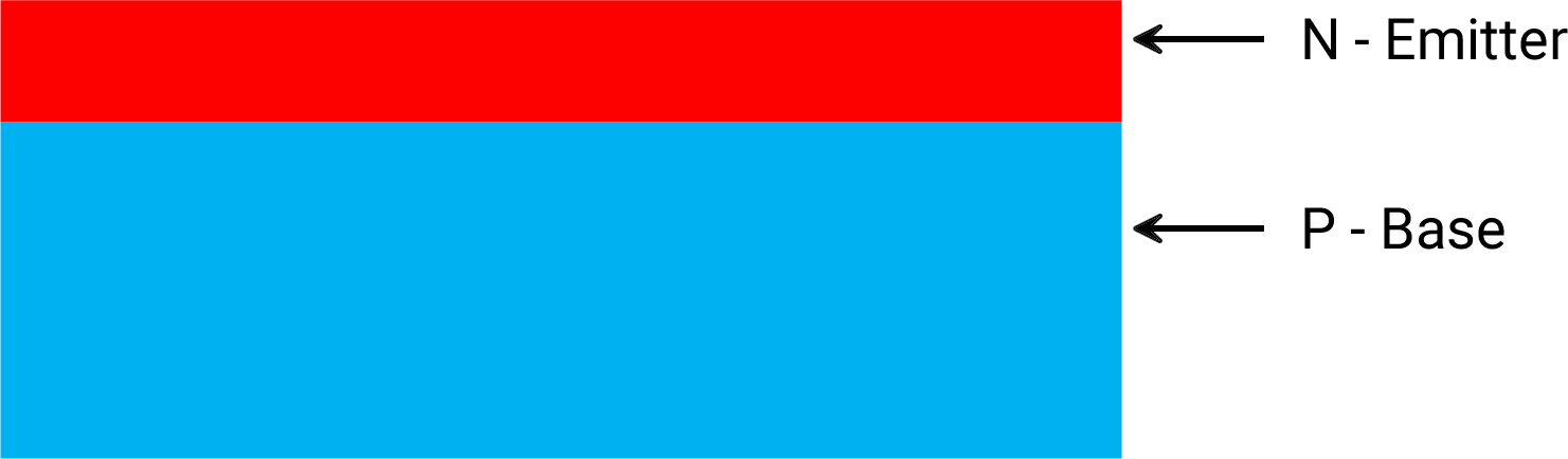
Figure 1: Example – PV wafer after doping
Why Use Delcom to Measure the Sheet Resistance of Wafers
It is important to note that because eddy current meters rely on a magnetic field to achieve their reading, they have a number of advantages over four-point probes to include:
- Is non-destructive
- Reads through insulating layers
- Measures moving material
- Provides nearly instantaneous readings
- Provides real-time process inspection
Process-Specific Employment Strategies for Delcom Sensors
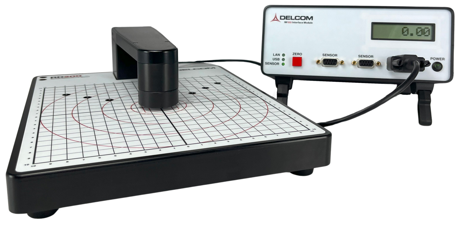
Eddy current sensors can be used in a straight-forward way to measure the sheet resistance of bulk doped wafers. Simply insert the wafer into the sensor’s magnetic field and observe the reading.
Figure 2: Measuring sheet resistance of bulk doped wafer

Eddy current sensors, use a magnetic field to inductively couple with the conducting layer of any material being measured. As such, any material placed within the field of an eddy current sensor will be measured even if the material is made of various layers separated by insulating layers. The sheet conductance of the entire stack is the sum of the sheet conductance of each layer – this phenomena is call superposition.
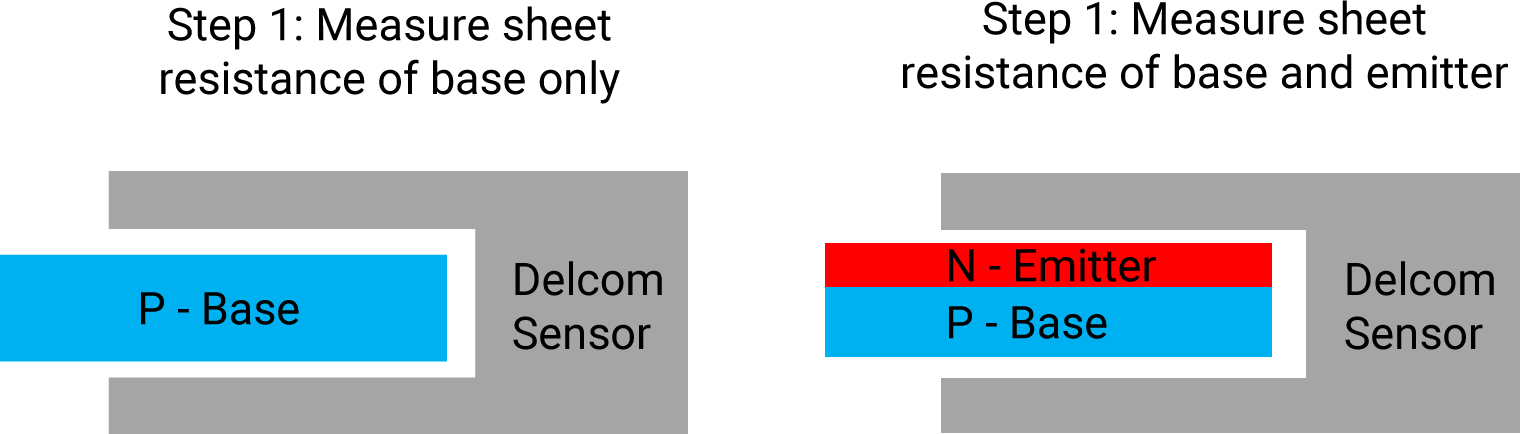
Therefore, in order to ascertain the sheet resistance of a bulk intrinsic doped wafer that was further processed to have a second extrinsic doped layer, the user must first measure the sheet resistance of the bulk doped wafer before the creation of the second doped layer. Then, after the creation of the second doped layer, the wafer is measured again. The sheet conductance of the second doped layer is merely the sheet conductance of the second reading minus the sheet conductance of the first reading. To get to sheet resistance, the sheet conductance need only by inverted. This is called the eddy current two-step process.
Eddy current two-step process:
- Step 1: measure the wafer prior to creation of second doped layer
- Step 2 measures the wafer after creation of second doped layer
Figure 3: The two-step eddy current method
Inline Sensor Deployment Strategy for Delcom Sensors
In general, Delcom sensor deployment strategies can include one or more of the following deployment tactics.
|
Deployment Strategy |
Image | Advantages |
|---|---|---|
| Single sensor single spot |  |
|
| Two sensors monitoring downstream | 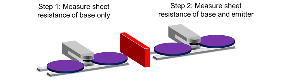 |
|
Recommended Sensors
Delcom recommends the following sensors based on the user’s material, stage of development, and application.
| Use case | Image | Recommended Sensor | Use case |
|---|---|---|---|
| Benchtop |  |
RD200 |
|
| Benchtop |  |
RS200 |
|
| Benchtop |  |
RD300 |
|
| Benchtop |  |
RS300 |
|
| Benchtop | 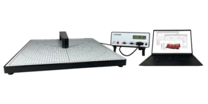 |
RD450 |
|
| Benchtop | 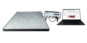 |
RS450 |
|
| Inline | 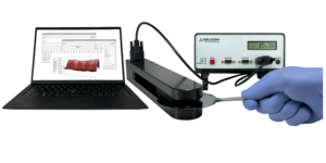 |
20J3 Hybrid |
|
| Inline | 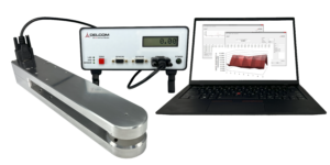 |
20J3 Inline |
|
| Inline | 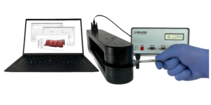 |
30C9 Hybrid |
|
| Inline | 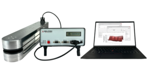 |
30C9 Inline |
|
| Inline | 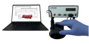 |
S3 Hybrid |
|
| Inline |  |
S3 Inline |
|
| Inline | 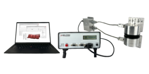 |
OEM |
|
| Inline | 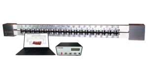 |
Multisensor |
|
Recommended Delcom Sensor Range
A specific resistivity is needed depending on the application for which the material is being produced. Measuring the resistivity of a wafer is quite difficult for a number of reasons to include the difficulty of working with a disc-shape, establishing perfect contact, etc. So, wafer researchers and manufactures instead measure sheet resistance. Sheet resistance is a measurement of per unit surface area. It does not present the difficulties of measuring resistivity yet still accomplishes the task – measuring the resistance to current flow and movement of electron and hole carriers in the wafer or layer of a wafer.
Typically for an n or p doped silicon wafer, sheet resistance ranges from .05 ohms/square to 5,000 ohms per square.
Figure 4: typical sheet resistance target values by common applications
| Product | Material | Target sheet resistance in ohms/square | Low sheet resistance in ohms/square | High sheet resistance in ohms/square |
|---|---|---|---|---|
| All | n or p doped wafer | .05 | 5000 | |
| LED | n-type cladding layer in GaN and Sapphire wafer | |||
| Crystalline PV solar cell | n-type emitter layer | 70 | 90 | |
| Integrated Circuits (ICs) | Boron p-type dopant | |||
| Power devices | Antimony n-type dopant |
Delcom sensors measure sheet resistance. Delcom makes sensors in four ranges – each range able to measure a different range of sheet resistances. When considering which sensor is right for a particular application, the right range of instrument must be selected based on the target sheet resistance of the material.
Figure 5: Delcom’s sensor ranges:
| Range Name | Min Sheet Resistance in ohms/square | Max Sheet Resistance in ohms/square |
|---|---|---|
| x10 | 5 | 100000 |
| x1 | 0.5 | 10000 |
| ÷10 | 0.05 | 1000 |
| ÷100 | 0.005 | 100 |
Typically for an n or p doped silicon wafer, sheet resistance ranges from .05 ohms/square to 5,000 ohms per square.