 Veteran Owned
 Veteran Owned
Printed Electronics
What is Measured
Printed electronics are materials that have electrical or electronic characteristics and were created using one or more printing techniques. Delcom sensors are widely used in this industry to characterize the sheet resistance, electrical performance, and thickness of conductive layers and structures.
Delcom sensors are compatible with any number of printing techniques/technologies to include:
- Inkjet printing
- Screen printing
- Aerosol jet printing
- Evaporative printing
Figure 1: Printed electronics – generic printing process
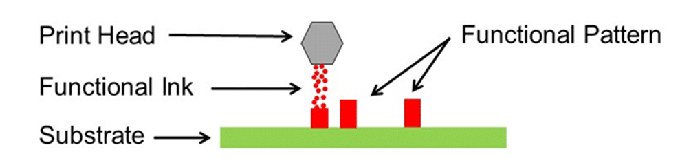
A conductive ink is usually a thermoplastic pasted consisting of the functional part of the ink (usually a conductor), a binder, a solvent, and a surfactant. The Delcom sensor measures the functional part of the ink which is often comprised of: (credit to: https://www.sigmaaldrich.com)
- Conductive Inks
- Metal nanoparticle and microparticle inks
- Silver (Ag) based pastes and colloidal
- Gold (Au)
- Platinum (Pt)
- Copper (Cu)
- Nickel (Ni)
- Conducting polymer-based inks
- Carbon nanomaterial based conductive inks
- Metal nanoparticle and microparticle inks
- Semiconductor Inks
- Conventional inorganic based semiconductor inks
- Metal oxide
- Organic semiconductor inks
- Conventional inorganic based semiconductor inks
- Dielectric Inks
- Organic polymers
- Ceramics in solvents
- Insulating 2D nanomaterials such as hexagonal boron nitride
- Insulators
Delcom sensors are usually employed to measure the functional component of the ink once it has been applied to the substrate. Common substrates include:
- Glass
- Silicon
- Flexible Paper
- Flexible foil
- Polyethylene terephthalate (PET)
- Plastic film
- Fabric
- Metals
- 3D printed objects
Why Measure with Delcom
The printed electronics industry has significant challenges to overcome to realize its full potential. Not least of which is durability, reliability, resolution all while decreasing resistance (of conducting elements) and keeping manufacturing costs low. Delcom sensors area employed all along the research to production continuum — to include R&D, pilot production, full-scale manufacturing, and product certification/qualification – to help address and overcome these many challenges.
Many printed electronics consist of patterns and there is a need for feedback regarding whether the pattern was printed correctly and in the correct location – this often confirmed using visual or optical metrology. But, to dig a little deeper, the printed electronic pattern has a shape and thickness. If this pattern is conductive or semiconductive it has a purpose the is electrical in nature.
Currently, in order to measure the electrical performance of a particular pattern, the production line must be stopped, a portion of the pattern removed, conductive points attached to the pattern, and current run through the pattern. This method has many drawbacks to include
- Possibly destroying the sample
- Possibly stopping a line mid-run
- Significant time to mount a batch on a wind/rewind to find samples to test
- Manual time-consuming process
- Occurs after a batch is produced which will result in waste of the whole batch as its too late to correct the manufacturing process, and
- It’s nearly impossible to certify 100% of the product.
Delcom sensors offer the following advantages static contact testing of printed electronics to include:
- Is non-destructive
- Reads through insulating layers
- Measures moving material
- Provides nearly instantaneous readings
- Provides real-time process inspection
- Not impeded by texture or patterns
Employment Strategies
A common question that must be answered by researchers designing conductive ink, innovators created products using printed electronics, and manufacturers monitoring conductive printing processes is where in the production process to measure the sheet resistance of the printed electronic structure.
A major issue to contend with involves the tendency of conductive inks to change their sheet conductance as they cure/dry.
Figure 2: Example of sheet resistance deterioration during curing (Credit Novacentrix)
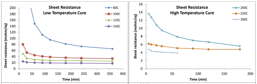
Knowing the sheet resistance deterioration based on curing temperature curve is critical when determining when in the process to monitor the conductive material. Delaying measurement until after the ink is fully cured could result in a delay in identifying issues with the production process and result in lost time and material.
Delcom sensors can be employed immediately after the application of the conductive ink and again after the curing process. Simple association can be used to determine what sheet resistance in the application stage correlates with the target sheet resistance of the final product. And, – of course – this can be done inline and at -speed.
Cross-Web & Downstream Monitoring
In general, Delcom sensor deployment strategies can include one or more of the following deployment tactics.
|
Deployment Strategy |
Image | Advantages |
|---|---|---|
| Single sensor single spot |  |
|
| Two sensors monitoring cross-web |  |
|
| Two sensors monitoring downstream | 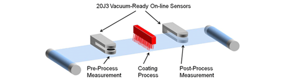 |
|
| Multi-channel monitoring cross-web | 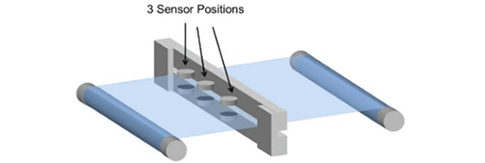 |
|
Recommended Sensors
Delcom recommends the following sensors based on the user’s material, stage of development, and application.
| Use case | Image | Recommended Sensor | Use case |
|---|---|---|---|
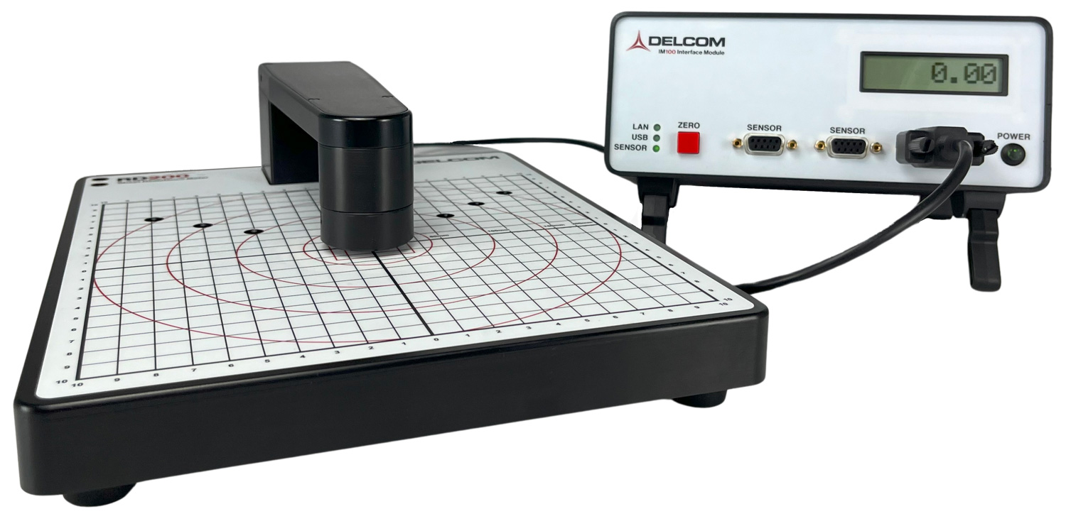
| Benchtop | 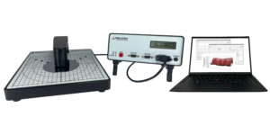 |
RD200 |
|
| Inline |  |
20J3 Hybrid |
|
| Inline |  |
20J3 Inline |
|
| Inline |  |
OEM |
|
| Inline | 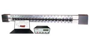 |
Multisensor |
|
Recommended Sensor Range
Delcom sensors measure sheet resistance. Delcom makes sensors in four ranges – each range able to measure a different range of sheet resistances. When considering which sensor is right for a particular application, the right range of instrument must be selected based on the target sheet resistance of the material.
Figure 3: Delcom’s sensor ranges:
| Range Name | Min Sheet Resistance in ohms/square |
Max Sheet Resistance in ohms/square |
|---|---|---|
| x10 | 5 | 100000 |
| x1 | 0.5 | 10000 |
| ÷10 | 0.05 | 1000 |
| ÷100 | 0.005 | 100 |
Delcom products measure sheet resistance which is – of course – a function of the thickness and bulk resistivity of the conductive ink. Thickness is often limited by the printing process – for example, with silver flake ink, the manufacturer usually will not want to go much thicker than 125 to 150 microns wet which dries to 40 microns thick. So, if the sheet conductance of the material (or the conductance of the trace) are insufficient, creating a thicker film is not acceptable, the manufacture would need to move to a more conductive ink
Figure 4: typical sheet resistance target values by common applications
| Product | Ink | Substrate | ρ (Resistivity) in ohm-cm | Target sheet resistance in ohms/square | Target thickness in micrometers |
|---|---|---|---|---|---|
| Battery Anodes | X.X × 10-6 | ||||
| RFID Tags |