 Veteran Owned
 Veteran Owned
Crystalline Solar
What is Measured
This paper pertains to the use of Delcom sensors to aid in the production of crystalline silicon solar to include:
- Monocrystalline silicon
- Epitaxial silicon
- Polycrystalline silicon
- Ribbon silicon
- Mono-like-multi silicon (MLM)
Delcom sensors will work with nearly all base wafer materials to include:
- Monocrystalline silicon – sawed from a single crystal boule
- Epitaxial silicon – grown on a “seed” wafer by chemical vapor deposition (CVD)
- Polycrystalline (aka: multicrystalline) silicon – smaller crystals that are grown, cast into an ingot then sawed into wafers
- Ribbon silicon
- Mono-like-multi silicon (MLM)
Why Measure with Delcom
Delcom sensors are used to monitor sheet resistance during or after the diffusion stage of production wafers in which phosphorus is diffused into a thin layer of the wafer surface.
Delcom sensors are used to prevent insufficient or excessive levels of doping. Such incorrect doping levels could result in insufficient ability to conduct away the generated electricity without resistive loses or reduce the quality of the material such that carriers recombine before reaching the P-N junction.
Sheet resistivity of a solar cell material is commonly measured because the magnitude of the resistivity directly affects cell performance The sheet resistance of this emitter is directly related to the density of the dopant which in turn determines:
- emitter saturation current density
- emitter quantum efficiency
- contact resistance properties
- tolerance to shunt formation during firing
Delcom sensors are used to monitor the dopant levels indirectly by continuously monitoring sheet resistance levels.
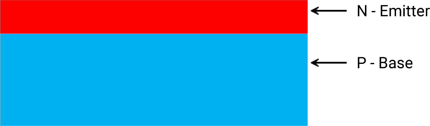
Figure 1: PV Wafer Stack
Employment Strategies
Eddy current sensors can be used in a straight-forward way to measure the sheet resistance of bulk doped wafers. Simply insert the wafer into the sensor’s magnetic field and observe the reading.
Figure 2: Measuring sheet resistance of bulk doped wafer

Eddy current sensors, use a magnetic field to inductively couple with the conducting layer of any material being measured. As such, any material placed within the field of an eddy current sensor will be measured even if the material is made of various layers separated by insulating layers. The sheet conductance of the entire stack is the sum of the sheet conductance of each layer – this phenomena is call superposition.
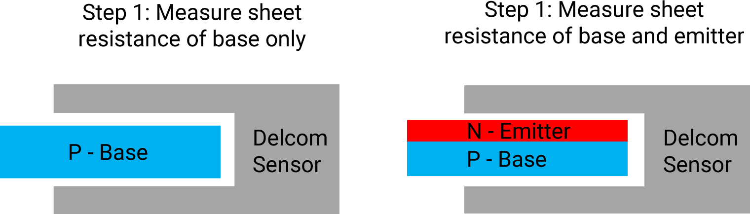
For this reason, in order to ascertain, the sheet resistance of the emitter layer, the user must first measure the sheet resistance of the base layer before the creation of the emitter layer. Then, after the creation of the emitter layer, the wafer is measured again. The sheet conductance of the emitter layer is merely the sheet conductance of the second reading minus the sheet conductance of the first reading. To get to sheet resistance, the sheet conductance need only by inverted. This is called the eddy current two-step process.
Eddy current two-step process:
- Step 1: measure the wafer prior to creation of emitter layer
- Step 2 measures the wafer after creation of the emitter layer
Figure 3: The two-step eddy current method
The primary purpose of an inline eddy current sensor for silicon PV wafers is to measure the emitter layer. In order to accomplish this manufacturer must utilize the eddy current two step process.
- Step 1 occurs prior to creation of the emitter layer by diffusion. In this step, the wafers should be introduced to an eddy current sensing head via automation. Typically, wafers are removed from their cartridge and introduced into the eddy current sensor via a conveyor or an arm. The sheet resistance value of each wafer is recorded. Multiple readings can be taken on each wafer in less than a few seconds.
- Step 2 occurs after the diffusion process. Again, wafers are introduced into an eddy current sensor via motion control and a second reading is taken. The sheet conductance of the emitter layer is merely the sheet conductance of the second reading minus the sheet conductance of the first reading. To get to sheet resistance, the sheet conductance need only by inverted.
Cross-Web & Downstream Monitoring
In general, Delcom sensor deployment strategies can include one or more of the following deployment tactics.
|
Deployment Strategy |
Image | Advantages |
|---|---|---|
| Single sensor single spot | 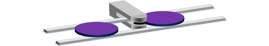 |
|
| Two sensors monitoring downstream | 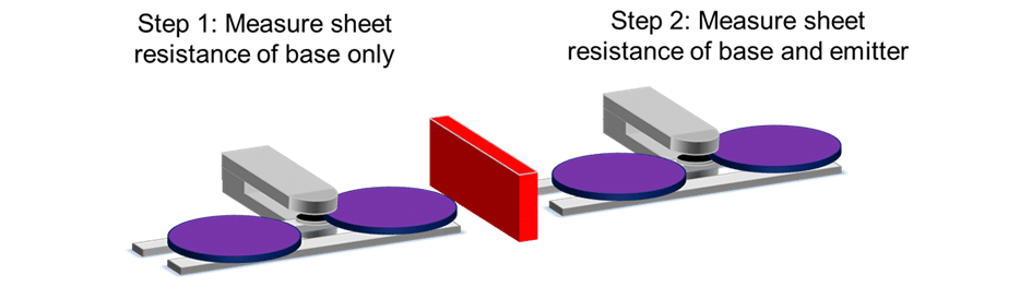 |
|
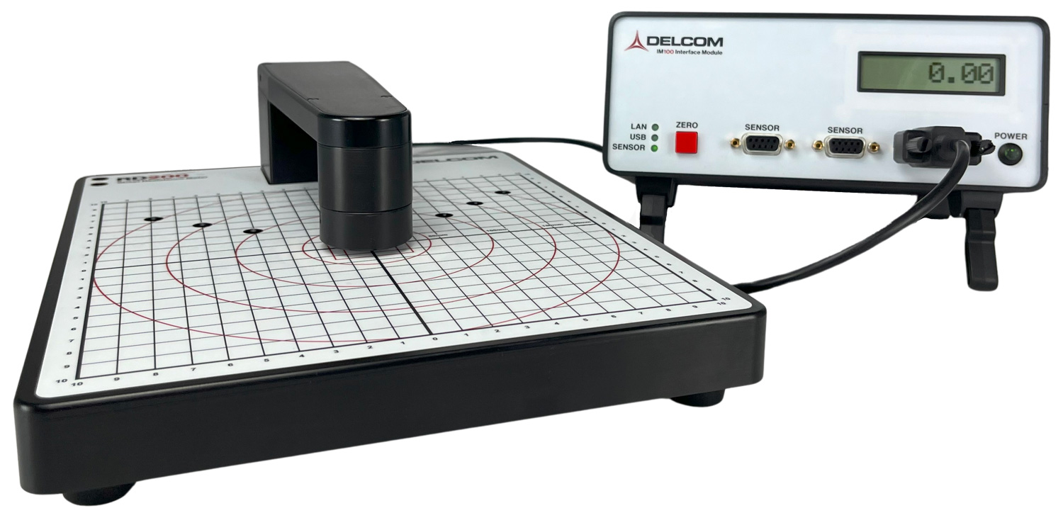
Recommended Sensors
Delcom recommends the following sensors based on the user’s material, stage of development, and application.
| Use case | Image | Recommended Sensor | Use case |
|---|---|---|---|
| Benchtop |  |
RD200 |
|
| Benchtop |  |
RD300 |
|
| Benchtop | 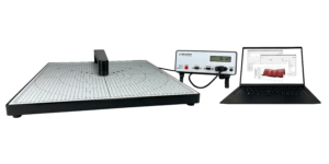 |
RD450 |
|
| Inline | 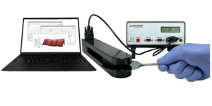 |
20J3 Hybrid |
|
| Inline | 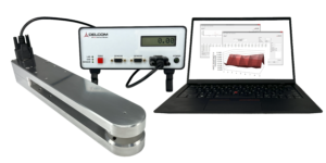 |
20J3 Inline |
|
| Inline | 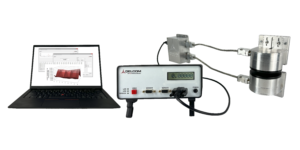 |
OEM |
|
Recommended Sensor Range
Delcom sensors measure sheet resistance. Delcom makes sensors in four ranges – each range able to measure a different range of sheet resistances. When considering which sensor is right for a particular application, the right range of instrument must be selected based on the target sheet resistance of the material
Figure 4: Delcom’s sensor ranges:
| Range Name | Min Sheet Resistance in ohms/square |
Max Sheet Resistance in ohms/square |
|---|---|---|
| x10 | 5 | 100000 |
| x1 | 0.5 | 10000 |
| ÷10 | 0.05 | 1000 |
| ÷100 | 0.005 | 100 |
For a typical three-bus-bar silicon solar cell, the emitter sheet resistance should be in the 70-90 ohms/square range. The recommended instrument range for this application is “x10”. The x10 range instrument can measure from 5 ohms/square to 100,000 ohms per square.
At the sheet resistance of 70 ohms/square – for example -, the instrument will provide four significant digits, meaning that it will be able to measure deviation from the target thickness by +/- 1%.